
 |
Thin Film System Features
|
|
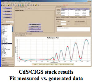
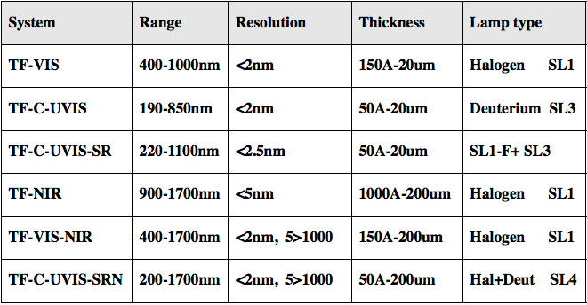
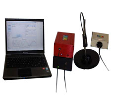
We offer a complete line of film thickness measurement systems that can measure from 5 nm to 200 µm for analysis of single layer and/or multilayer films in less than a second. StellarNet thin film reflectometry systems consist of a portable USB spectrometer coupled to a reflectance probe and light source. The optical properties are obtained from reflection and thickness is measured by detecting the sinusoidal fringe pattern from the sample's specular reflectance. Several spectrometer models are available to suit your thin film and/or optical measurement requirements. Increased production of Thin-Film Photovoltaics (TFPVs) is becoming more predominant due to lower costs than their silicon-wafer-based cousins. Getting the accurate thickness measurement is extremely crucial to efficiency and reliability as well as maintaining production costs. Films include active layers such as thin silicon, II-VI materials such as CdTe, and CIGS (copper indium gallium selenide). Additionally, TCO (transparent conductive oxide) stacks, polyimides and resists used to define cells and electrodes, as well as anti-reflection coatings can all be measured with StellarNet Thin Film Measurement systems.
StellarNet systems can measure thickness of non-metallic semiconductor process films. Also, StellarNet Thin Film Measurement systems can be used to locate and identify the cause of failure in integrated circuits. Systems are also used during MEMS patterning processes to measure photoresist thickness and uniformity. These systems are also being used during silicon etching to measure etch rate and membrane thickness and uniformity. Thickness measurement of thick polysilicon films and SOI are also common applications.
Polymer films such as PET and polycarbonate require monitoring of film thickness during manufacturing.Please contact us to discuss your application.
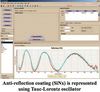
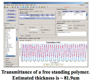
Most flat panel displays including LCD, OLED, and many other display technologies employ transparent conductive oxides (TCOs) to transport current and to each light emitting element of the display. StellarNet Thin-Film Measurement Systems can be used to measure thickness of Liquid Crystal layers such as polyamide, hardcoat, and air gap. And for OLED displays systems are able to measure layers such as emissive, injection, buffer, and the encapsulation layer. Optical coatings are used to enhance the reflectance and transmittance properties of a substrate material. StellarNet Thin-Film Measurement systems can be used to measure anti-reflection, increased reflection coatings, high-pass, low-pass, and band pass filters. StellarNet spectrometer systems also come with SpectraWiz Software for CIELAB colorimetry. See our colorimeter page. StellarNet Thin-Film Measurement Systems can be used to measure coatings on Ophthalmic Lenses. Spectral reflectance can be used to measure anti-reflectance coatings on lenses as well as hardcoat and hydrophobic layer thickness. StellarNet Thin-Film Measurement systems have been used to measure the thin metal films in various applications. Please contact us to discuss your application. Parylene and a variety of poly (p-xylylene) polymers are used extensively as moisture barriers and electrical insulators and their coating thicknesses can be measured via reflectance spectroscopy. Parylene applications included coatings for printed circuit boards and medical devices such as stents and pacemakers, permanently implanted in the body. Many industries use hardcoats and various protective coatings. Layer thickness and thickness monitoring is extremely important for manufacturing and quality control. Thick photoresists such as SU-8, a commonly used epoxy based negative photoresist normally spun in layers from 0.1um to 2mm. Monitoring of thickness can be crucial during production and fabrication of multilayer stacks. Thickness and optical constants (n and k) can be measured quickly and easily using powerful user-friendly software which make daily complex measurements quick and simple. TF software includes a large library of materials data that enables measurement of the wide range of layer structures: multilayer, freestanding, rough, thick and thin layer structures are supported. New materials can be added easily by measuring corresponding sample or importing data from the text file. The measurement process consists of two steps: data acquisition and data analysis. TF Systems defines all the process in a measurement recipe and makes it transparent to the user. At the same time the user has the ability to store measured data and analyze it later. TF supports Parameterized materials e.g. Cauchy, Sellmeir, EMA (effective-medium approximation), Harmonic oscillator, Tauc-Lorentz oscillator, Drude-Lorentz and many more approximations. These approximations represent optical dispersion of materials in desired spectral range using few coefficients that can be adjusted. For example, oxides are frequently represented using Cauchy and glasses using Sellmeir approximation, amorphous materials (e.g. SiNx, aSi) can be represented using Tauc-Lorentz and phase-mixed materials (e.g. poly-Si) using EMA approximation. Measurements are made using: reflectance/transmittance spectroscopy which measures the optical response of the layer structure. The user creates an optical model of the layer structure and uses data analysis to determine physical properties: the results are inferred from the best fit of measured and modeled data. TF software provides many options to easily analyze simple and most complex filmstacks, graded layers, periodic structures, very thick films, films on thin substrates, multi-sample measurements, etc. Simulation and error-estimator tools allow user better understand data and the expected precision. During in-situ, in-line or other long running measurements conditions like surface roughness, ambient light, etc. may be changing. TF software supports roughness and scaling correction that allows factoring in these effects. From most simple, routine measurements to multilayer, multi-sample analysis - our software is ready to help!
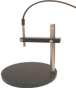
The Modbus server plug-in provides a communication interface over TCP IP. TF software is deployed as a server and supports external program integration. This allows user to send a measurement request from any program and receive back the thickness results data. R600 Reflectance Probe has both illumination and read fibers bundled together coupling to the system. The new, improved reflectance probe holder allows for variable distance from sample.
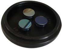
TF-STD1Thin Film standards for thickness measurement verification. Includes Si substrate for reference with 2 additional SiO2 substrates - 100nm and 1000nm thickness.
Portable spectrometers include a USB-2 interface cable and interface to any 32-bit pc for a portable or tabletop measurement system.
Vacuum deposition is a family of processes used to deposit layers atom-by-atom or molecule-by-molecule at sub-atmospheric pressure on a solid surface. The layers may be as thin as one atom to millimeters thick (freestanding structures). There may be multiple layers of different materials (e.g. optical coatings). A thickness of less than one micrometer is generally called a thin film while a thickness greater than one micrometer is called a coating. StellarNet Thin-Film measurement systems can be used to check deposition thickness of a wide range of materials. Please contact us to discuss your application.
|
|
|
|
|
Nav view search
Navigation